MT6169 chip schematic diagram and data sheet download
MT6169 chip schematic diagram and data sheet download
There are a lot of development materials about the MT6169 chip, and only a small part has been sorted out. If you want more complete chip information, you can download it for free from the hacker.com technical forum. The full version of the development materials, design schematics and data sheets can also be added. Group acquisition: 813238832, I will never regret sharing it with you
Data link: https://bbs.usoftchina.com/thread-198789-1-1.html
Figure 1
Overview
The MT6169 is a multi-mode multi-band transceiver in 40nm CMOS. The RF transceiver functionality is fully integrated. In the overall product, this document describes the performance targets for the RF macros to be embedded.
key features
1. Full multi-mode RF solution (GG/WCDMA/TDSCDMA/LTE)
Multi-band LTE/WCDMA/TD-SCDMA/Quad-band GGE
16QAM UL/64 QAM DL(HSPA+/LTE)
2G/3G/4G co-band
RXD support (8 RXD ports)
2. Direct Conversion (LTE/3G), GMSK and Two-Point Modulation (TPM) for Small Signal Pole for 8PSK
Dedicated power detection circuit for power control of specific power ranges
3. Hybrid direct conversion (4G/3G)/low-IF (GGE, DC-HSDPA) receiver
4. Low supply current and work directly from DC-DC converter
5. 26MHz internal DCXO or external VCTCXO operation (with integrated AFC DAC)
Three low-noise additional clock drivers for clock connection/peripheral ICs
Ultra Low Power 32 kHz Mode
6. RF calibration features to support key Rx and Tx specifications (image rejection, LO feedthrough, DC offset
7. Temperature measurement subsystem
receiver
The direct conversion /LIF receiver (RX) contains all the active circuits used to support the entire receiver chain. LTE (TDD/FDD), Single Cell (SC)/Dual Cell (DC) 3G WCDMA, 3G TDSCDMA and 2G GSM/GPRS/EDGE (GGE) mode reception. This path contains a total of 8 LNAs (low noise amplifiers), 8 mixers, 8 LO dividers, I/Q currents. Buffers, I/Q LPF1 and I/Q LPF2 analog filters.
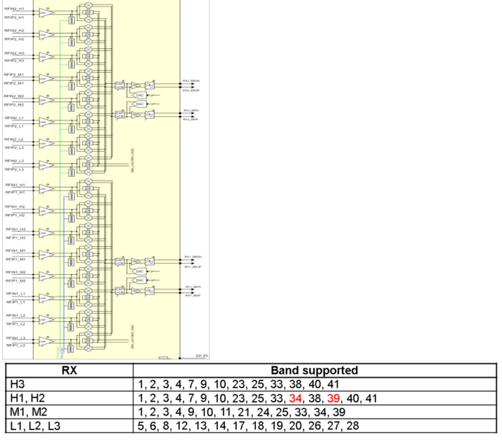
All LNAs have balanced inputs and are fully integrated. The quadrature LO signal is generated by the divider. for all LNAs. The RF signal is downconverted by a high/lowband quadrature downconversion mixer. This analog baseband filter is a low-pass filter with programmable transfer function and gain control. Additionally, it contains an RC calibration circuit and a DC offset cancellation circuit (DCOC). Receiver power on/off sequence, LNA/band selection, overall receiver gain including LNA, mixer and analog baseband and DCOC timing are controlled by digital circuitry. Additionally, IQ calibration is done by injecting offset frequency test tones. Generated by the Test Tone Generator (TTG) into the RX mixer. Additional leap IQ imbalance tracking may be added to the database without changing receiver design. The timing and control of the calibration scheme is also controlled by the L1 software and digital circuitry.