How to read the schematic diagram of the development board
How to read the schematic diagram of the development board
Take the schematic diagram of 100ASK_STM32F103 as an example to introduce how to read the schematic diagram. The reader only needs to grasp a few key points to understand the basic meaning of the schematic diagram. The schematic diagram of 100ASK_STM32F103 is in the "4_Hardware Information" folder. Readers can open "100ASK_STM32F103 Schematic Diagram.pdf" (hereinafter referred to as "Schematic Diagram") to read with this manual.
The "Schematic" has 11 pages in total. The first page contains the overall block diagram, catalog, and version information; the second page is the core of the development board - the schematic diagram of STM32F103ZET6; the third page is the minimum system of the microcontroller, including MCU power, clock, Reset, etc.; the fourth page is the system power supply; starting from the fifth page, is the schematic diagram of each module, when programming a module, you need to find the corresponding part to view. That is to say, we can focus on the first 4 pages at present, so that after the split, the overall framework will be clearer.
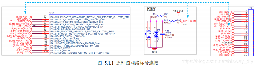
In the schematic diagram, in addition to using a connection line to indicate that the two devices are connected, network labels are often used to indicate the connection. As shown in Figure 5.1.1, the red text is the network label, as long as the two network labels are the same, it means they are connected. On the schematic diagram, KEY1 appears three times in total, which are the 34-pin of MCU on the second page, the button 1 module on the fifth page, and the 15-pin of the expansion pin header J21 on the eleventh page. They indicate that they are electrically connected, and the corresponding physical objects That is, the 34-pin of the MCU is connected to the button 1, and is led out through J21 at the same time.
There is "{5,11}" in front of KEY1 on the second page, which means that there are KEY1 on pages 5 and 11 in addition to this one. Similarly, there is "{2,11}" in KEY1 on page 5, which means that there are KEY1 on pages 2 and 11 besides this one. Readers can quickly understand how many times the network label appears and where it appears through this identification.
There are many types of devices on the schematic diagram, but still follow the "28 principle", 80% of which are common devices, so we only need to be familiar with common devices. Each type of device is usually marked with an abbreviated English name. For example, a resistor is usually marked with Rn (n is a number). Common components are shown in Table 5.1.1 below.
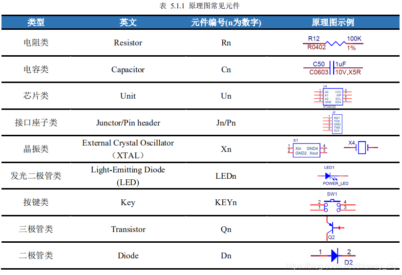
For resistors and capacitors, there are a large number of devices with different specifications. In addition to the part number, there is usually information such as value, package, properties, etc. For example, the resistance R12 in the above example has a resistance value of 100KΩ, the package is 0402, and the accuracy is 1%. The capacitor C50 in the above example has a capacitance value of 1uF, the package is 0603, and the withstand voltage is 10V. X5R indicates that it works in the temperature range of -55℃~+85℃, and the capacitance deviation is less than ±15%. For embedded software engineers, it is usually only concerned with the component number and the resistance/capacitance value.
For a single-chip microcomputer system, the minimum system function should be guaranteed first, and then the control or data transmission with each peripheral module should be realized. Therefore, looking at the schematic diagram, the first focus is on the smallest system, followed by each peripheral module. For the peripheral circuit of the peripheral module, what power supply is needed, how to wire it, and how to set the value of the resistor/capacitor, the reader does not need to worry too much, usually can find the reference circuit, and then check it carefully according to the chip manual, and finally debug and verify it.
[Summary]
When analyzing the minimum system of STM32 later, you can feel how to analyze the details of the schematic diagram. For the basic part of the schematic diagram, the reader
can temporarily understand the following content:
- Sort out the schematic block;
- understand network labels;
- Familiar with common components;
- Understand the properties of resistance and capacitance;
Baiwen Technology Forum:
http://bbs.100ask.net/
100ask Embedded Video Official Website:
https://www.100ask.net/index
Baiwen development board:
Taobao: https://100ask.taobao.com/Tmall
: https://weidongshan.tmall.com/
Technical exchange group (Hongmeng development/Linux/embedded/driver/data download)
QQ group: 869222007
SCM-Embedded Linux Exchange Group:
QQ Group: 536785813