联发科技MT6166芯片资料汇总 ,MT6166开发设计参考
联发科技MT6166芯片资料汇总 ,MT6166开发设计参考
今天分享MT6166数据表的部分资料,供大家学习和工作中参考,资料比较齐全,只分享以下的部分资料
MT6166概述
MT6166是以高速2G/3G-FDD/TDD多模式智能手机为目标的射频收发器。平板电脑植入40nm CMOS。RF收发器功能完全集成。MT6166为基带芯片,用来合成即将发射的基带信号,或对接收到的基带信号进行解码
这是一个PLL,用于产生某些校准模式的测试音。
1、用于图像抑制校正的接收机输入反馈
2、对功率探测器PIN(PDET)的反馈作为接收机增益校准的校准音调
此外,该PLL还产生用于其他目的的时钟:
1、TX动态数字26M时钟。
2、26M用于TX检测ADC。
3、216TX数据通道416M。
4、104m的RC CAL。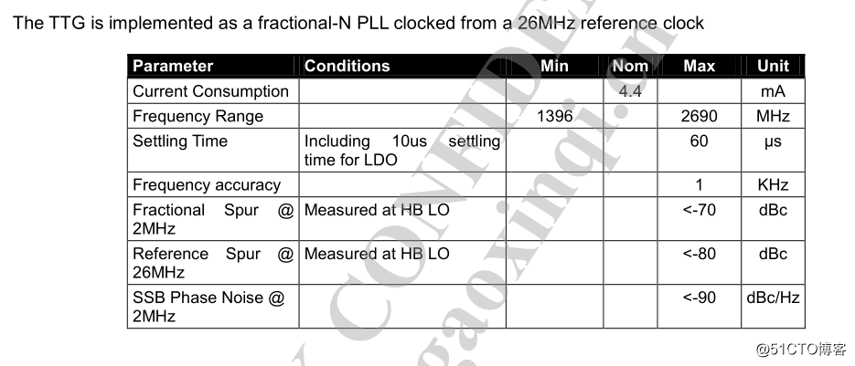
图一
MT6166接收机:
直接转换/LIF接收机包含支持单接收器的全部接收器链的所有有源电路。小区(SC)/双小区(DC)3G WCDMA、3G TDSCDMA和2G GSM/GPRS/EDGE(GGE)模式接收。这个路径包含总共7个LNA(Low Noise Amplifier)。前4个LNA支持3G BAND1/2/3/4/5/6/8/9;第五LNA支持TDD B40;最后2个LNA支持GGE低频带(GSM850/900)和GGE高频带(DCS1800/PCS1900)。GGE高频段低噪声放大器也支持TDD B33/B34/B39。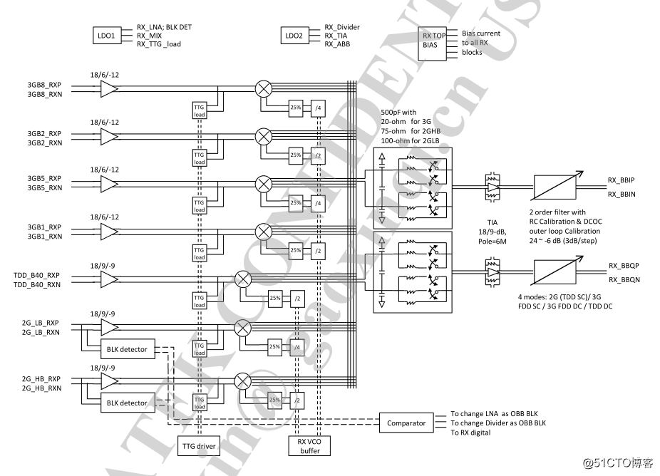
图二
接收器也可用于支持双通话操作的平台中。在双对话应用程序中,前4个LNA还通过联合显带来支持TDD B33/B34和2G带。如表中列出的,有8个单会话和双对话应用场景。3线控制用于选择这些方案中的一种正常操作。所有的LNA都有平衡的输入,并且是完全集成的。正交LO信号是由分频产生的。
MT6166芯片资料,设计原理图和设计表的更多资料可以在U创技术论坛可以找到下载:
原文链接:https://bbs.usoftchina.com/forum-258-1.html
图三
A BY-2 divider for high-band (HB) LNAs and a divide-by-4 divider for low-band (LB) LNAs. The RF signal is
a downconverted high/lowband quadrature direct downconversion mixer. Analog baseband filters are low-pass filters with programmable transfer functions and gain control. Additionally, it contains an RC calibration. circuit and DC offset cancellation circuit (DCOC). The low-pass filter is configured as a second-order North Sea. Filters for 3G FDD SC, 3G FDD DC, TDD DC and GGE modes. Receiver power on/off sequence, LNA/band selection, total receiver gain including LNA, mixer and analog baseband and DCOC timing by digital circuitry. Additionally, IQ calibration is done by injecting test tones at offset frequencies generated by the test.
The tone generator (TTG) goes to the RX mixer. Additional IQ imbalance tracking can be added in the DB. without changing the receiver design. The timing and control of this calibration scheme is also controlled by L1. software and digital circuits.